
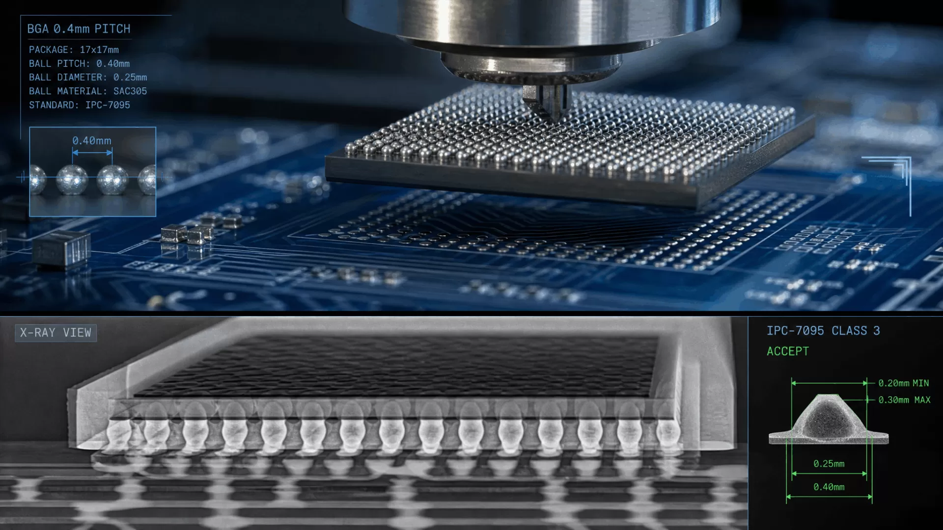
Ball grid array packaging has transformed PCB design by packing hundreds or thousands of interconnects into a footprint that would accommodate only a few dozen leads in a QFP. But this density comes at a cost that is invisible: every solder joint under a BGA is hidden from optical inspection. A board that passes automated optical inspection with zero defects can still fail in the field because of voids, head-in-pillow opens, or insufficient solder collapse beneath a BGA that no camera can see. ADD Components addresses this fundamental quality gap with a comprehensive BGA assembly capability that spans 0.4 mm-pitch micro-BGAs through to large-body packages up to 55 x 55 mm, supported by in-line X-ray inspection on every production lot and reflow profiling engineered to the specific thermal mass of each BGA device.
The Hidden-Joint Problem and Why X-Ray Is Not Optional
A 1,156-ball BGA on a 1.0 mm pitch presents 1,156 potential failure points, every one of them optically inaccessible after reflow. The failure modes are well documented in IPC-7095: voids that grow during thermal cycling until they bridge adjacent balls or crack the joint; head-in-pillow defects where the solder paste wets the pad and the ball wets the flux but the two never fully coalesce; and non-wet opens where a contaminated ball surface prevents metallurgical bonding entirely. None of these defects can be detected by visual inspection, and electrical test alone often misses marginal joints that pass at room temperature but open under thermal expansion.
ADD Components operates automated X-ray inspection systems with sub-10-micron resolution capable of generating both 2D transmission images and computed-tomography slice views at any plane through a BGA joint array. Voids as small as 5 percent of joint cross-sectional area are detectable, well below the IPC-7095 Class 3 threshold of 25 percent maximum void size for a single ball and 15 percent for the package average. For every BGA-bearing assembly, a statistically sampled set of devices undergoes full void analysis with results reported against IPC-7095 criteria. Where customer specifications demand it, 100 percent X-ray inspection is available.
Placement Precision: From 0.4 mm Pitch uBGA to 0201 Passives
The placement accuracy required for fine-pitch BGA assembly exceeds that of standard SMT by a wide margin. A 0.4 mm-pitch micro-BGA — commonly used for mobile processors, FPGAs, and high-speed memory interfaces — has solder ball diameters of approximately 0.25 mm on pads of similar dimensions. The placement window is approximately 75 microns, meaning the placement system must achieve repeatability significantly better than this to maintain process capability above 1.33 Cpk. ADD Components uses high-speed pick-and-place systems with vision centering on every component, achieving placement accuracy of 35 microns at three sigma. Before placement, BGA components are inspected for missing, deformed, or oxidized balls, and the solder paste deposit is verified via solder paste inspection with volumetric measurement of every deposit on fine-pitch pads.
This same placement precision extends to the full range of fine-pitch surface-mount devices: 0.4 mm and 0.5 mm-pitch QFPs, QFNs with exposed thermal pads, 0201 chip components, and leadless packages such as DFNs and LCCs. The placement system's force-control mechanism limits Z-axis placement pressure to prevent solder paste smearing on ultra-fine-pitch pads, a common defect mode that produces bridging invisible to pre-reflow inspection.
Reflow Profiling for BGA Assemblies
Reflow soldering a BGA is fundamentally a heat-transfer problem with non-uniform boundary conditions. The outer balls of the array reach soldering temperature before the inner balls because they are closer to the convection flow. The package body acts as a thermal mass that slows heating of the die-attach region directly above the center of the ball array. And the PCB itself — particularly on multilayer designs with heavy copper planes — draws heat away from the BGA footprint, creating a temperature delta between the package and the board that must be carefully managed to avoid warpage-induced opens.
ADD Components develops a unique reflow profile for each BGA type on each board design. Thermocouples are bonded to balls at the corner, edge, and center of a sacrificial BGA, with additional thermocouples on the PCB surface adjacent to the package. The reflow oven's 10 independently controlled zones are tuned to produce a thermal profile in which the maximum temperature difference across the BGA ball array does not exceed 5 degree Celsius. Ramp rates are limited to 1.5 to 2.5 degree Celsius per second, and time above liquidus is held to 60 to 90 seconds — long enough for complete solder collapse and intermetallic formation but short enough to avoid excessive intermetallic growth that embrittles the joint.
For large-body BGAs — packages of 35 x 35 mm and above used in FPGA and network-processor applications — the thermal challenge intensifies. The CTE mismatch between the silicon die and the organic substrate causes the package to warp during heating, with the degree of warpage proportional to package size. Peak temperatures are carefully controlled to keep warpage within the solder paste's collapse tolerance, and cooling rates are managed to prevent warpage reversal from cracking joints before they fully solidify.
Void Prevention and Control
Voids in BGA solder joints originate from volatile compounds trapped in the solder paste flux that cannot escape before the solder solidifies. Their formation is influenced by solder paste chemistry, stencil aperture design, reflow profile, and the outgassing characteristics of the PCB laminate. ADD Components controls void formation through several concurrent strategies. Solder paste is selected for low-voiding formulations with optimized flux chemistry, and stencil apertures are designed with geometries that provide escape paths for volatiles — typically square apertures with rounded corners for BGA pads, as circular apertures under BGAs can trap flux volatiles at the aperture center. The reflow soak zone is extended to allow gradual volatile evolution before the solder reaches liquidus, and nitrogen-atmosphere reflow is used where necessary to improve wetting and reduce oxide-related void nucleation.
For designs requiring void levels below IPC-7095 Class 3 thresholds — increasingly common in automotive, aerospace, and high-reliability industrial applications — ADD Components offers vacuum-assisted reflow, where the soldering chamber is evacuated during the liquidus phase to mechanically extract gas bubbles from molten joints. This process routinely achieves void percentages below 5 percent across the entire BGA array.
| BGA Capability | Specification | Applicable Standard |
|---|---|---|
| Minimum Pitch | 0.4 mm (uBGA/CSP) | IPC-7095 |
| Maximum Package Size | 55 x 55 mm | IPC-7095 |
| Placement Accuracy | 35 um at 3-sigma | IPC-9850 |
| X-Ray Resolution | Sub-10 um | IPC-7095 |
| Void Detection Threshold | 5% joint cross-section | IPC-7095 Class 3 |
| Max Temperature Delta | 5 C across BGA array | Internal process spec |
Underfill and Mechanical Reinforcement
BGAs in products subject to mechanical shock, vibration, or repeated thermal cycling — handheld instruments, automotive engine-compartment modules, aerospace avionics — benefit from underfill encapsulation. Underfill is a low-viscosity epoxy that flows under the BGA after reflow, filling the gap between the package and the PCB and bonding to both surfaces. Once cured, it redistributes mechanical stress away from the solder joints and into the bulk epoxy, dramatically increasing thermal-cycle life. ADD Components applies underfill using precision dispensing systems with volumetric control, pre-heating the board to reduce epoxy viscosity and ensure complete capillary flow under packages as large as 45 x 45 mm. Corner-bond and edge-bond techniques are also available for applications where full underfill is unnecessary but additional mechanical retention is desired.
Reballing and Rework Capability
BGA rework presents challenges that distinguish it from simpler SMT rework: the package must be heated uniformly to avoid warpage, all joints must reach liquidus simultaneously for clean removal, and residual solder must be removed from the pads without damaging the solder mask or lifting pads from the laminate. ADD Components operates BGA-specific rework stations with programmable bottom-side pre-heaters, split-optics alignment systems, and closed-loop thermal control capable of following reflow profiles matched to the original assembly profile. After removal, pads are dressed using controlled vacuum desoldering, and replacement BGAs — either customer-supplied or sourced through ADD Components' distribution network — are placed, reflowed, and X-ray inspected. For components where only a subset of balls show damage, reballing services are available: the damaged balls are removed, the package underside is cleaned to remove residual solder and flux, and new solder spheres are applied using a precision stencil-and-reflow process.
Integrated Sourcing for BGA Components
High-density BGAs — FPGAs from Xilinx and Altera, processors from STM and TI, and memory devices from Microchip and others — are often the longest-lead-time items on a bill of materials. Allocation cycles can extend delivery to 52 weeks or more. ADD Components' position as a Hong Kong electronic components distributor with established supply relationships across all major BGA semiconductor manufacturers provides a sourcing pathway that standalone assembly houses cannot offer. BGA components can be procured alongside the assembly service, with inventory held at our Hong Kong logistics center and released to production against firm orders. This unified supply chain reduces the risk of production delays caused by misaligned component and assembly lead times.
Submit your BOM and Gerber files to info@addcomponents.hk for a PCBA quotation — typically within 24 hours.