
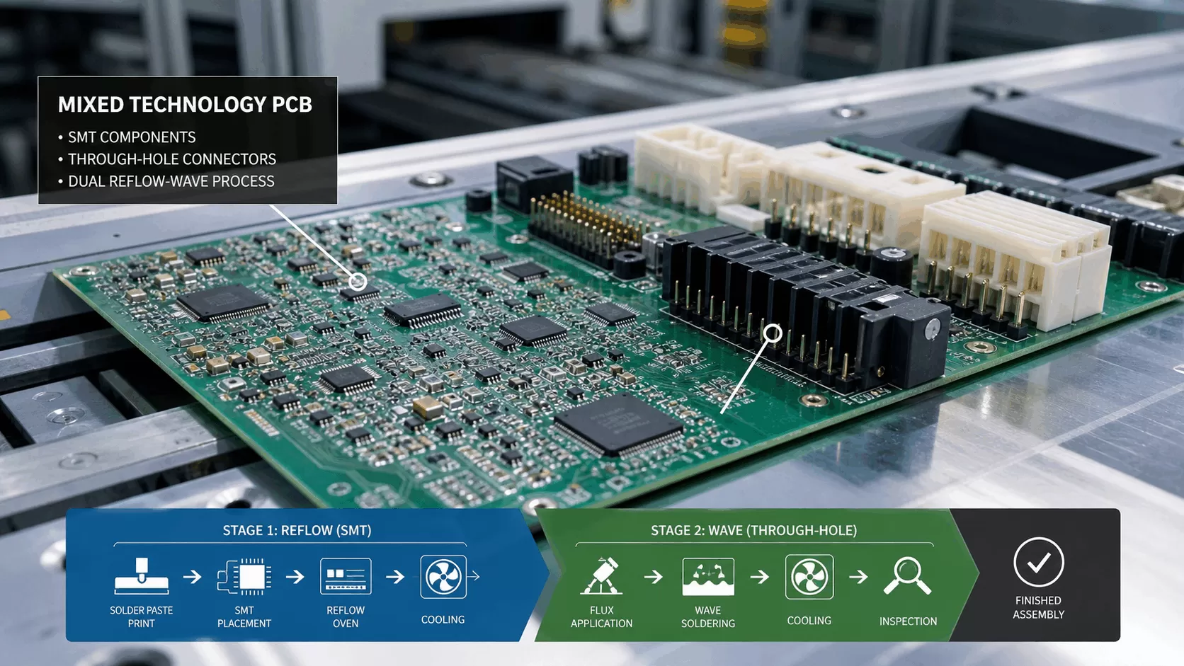
Few production challenges expose the gap between design intent and manufacturing reality as starkly as mixed-technology boards. On paper, combining a high-density BGA processor with through-hole power connectors and board-edge I/O appears routine. On the factory floor, the same board demands that two fundamentally different soldering processes — reflow for surface-mount devices and wave or selective soldering for through-hole components — be sequenced without damaging either population. ADD Components has refined its mixed-technology assembly workflow over more than two decades of serving industrial, telecommunications, and automotive electronics customers, developing process recipes that eliminate the thermal and mechanical conflicts inherent in hybrid boards.
The Process-Sequence Problem
The central challenge of mixed-technology assembly can be stated simply: solder melts. A reflow oven brings an entire board assembly to temperatures between 235 and 250 degree Celsius. A wave solder machine subjects the bottom side of a board to a molten solder wave at approximately 260 degree Celsius. If through-hole components are inserted before the SMT reflow step, their plastic bodies may deform, their internal connections may degrade, and their leads may oxidize in the reflow atmosphere. If SMT components are placed on the bottom side before the board passes through a wave solder machine, they will be immersed in molten solder and either detach from their pads or suffer catastrophic thermal damage.
Resolving this requires a strictly enforced process sequence, and ADD Components approaches every mixed-technology order with a documented process flow review before the first component is placed. The sequence decision tree considers board topology, component temperature ratings, solder joint accessibility, and the number of SMT and through-hole sides. For the majority of mixed-technology designs, the optimal sequence follows the industry-standard dual reflow-wave path, executed with careful thermal profiling at each stage.
Standard Mixed-Technology Process Flow
Stage 1: Top-Side SMT Placement and Reflow
The process begins with the side carrying the majority of surface-mount components — typically the topside. Solder paste is applied through a laser-cut stainless-steel stencil, with aperture geometries optimized for fine-pitch QFPs, BGAs, and chip-scale packages down to 0201 size. Automated pick-and-place machines populate all SMT positions at placement rates exceeding 40,000 components per hour, with vision centering on every placement to ensure alignment accuracy within 35 microns at three sigma. The populated board then passes through a 10-zone convection reflow oven, where the thermal profile is tuned to the most thermally demanding component on the board — often a large BGA or a ceramic-packaged device — with ramp rates controlled to under 3 degree Celsius per second to avoid component cracking from moisture-induced popcorning.
Stage 2: Bottom-Side SMT and Second Reflow
If the design includes bottom-side SMT components — common in double-sided load designs for space-constrained products — the board is inverted and the process repeats. This second pass through reflow demands careful adhesive application or solder-paste tack force to hold bottom-side components in place against gravity. ADD Components applies a secondary thermal profile that does not disturb the previously reflowed top-side joints; the peak temperature on the top side is monitored with thermocouples bonded to representative joints to confirm that solder does not remelt during the second pass. For boards with heavy top-side components, specialized tooling supports the assembly to prevent warpage during the inverted reflow cycle.
Stage 3: Through-Hole Component Insertion
With all SMT reflow steps complete, through-hole components are inserted. Automatic axial and radial insertion machines handle standard-leaded devices — resistors, diodes, small capacitors — at rates up to 15,000 placements per hour. Larger or irregularly shaped parts such as connectors, transformers, relays, and terminal blocks are placed manually or with semi-automated assistance. Pin-in-paste technology, where solder paste is printed into through-holes during the SMT stencil step and reflowed simultaneously with SMT parts, is used where feasible to eliminate a separate soldering step for selected through-hole joints.
Stage 4: Wave or Selective Soldering
The final soldering stage applies either wave soldering or selective soldering, depending on board geometry. When all through-hole components reside on a single side and no bottom-side SMT components are present, wave soldering provides the most efficient path. The board passes over a dual-wave system with a turbulent primary wave ensuring penetration into dense connector pin fields and a laminar secondary wave forming consistent fillets. When bottom-side SMT components are present — the more common case — selective soldering is deployed. A programmable micro-fountain nozzle targets each through-hole location individually, applying flux and solder with millimeter precision while leaving surrounding SMT components untouched. This combination of processes completes the mixed-technology assembly without thermal compromise to either component population.
| Process Stage | Method | Key Control Parameter | Risk Mitigated |
|---|---|---|---|
| Top-Side SMT | Stencil print + reflow | Profile ramp rate<3 c=""> | Component popcorning, tombstoning |
| Bottom-Side SMT | Adhesive + inverted reflow | Top-side peak<200 c=""> | Top-side joint remelt, component drop-off |
| THT Insertion | Auto-insert + manual | Lead protrusion 1.5-2.5 mm | Insufficient hole fill, bridging |
| THT Soldering | Selective or wave | Solder pot temp 260 plus minus 5 C | Bottom-side SMT thermal damage |
Thermal Management Across Process Stages
Every thermal cycle a board endures during assembly accumulates stress in the laminate, the plated through-hole barrels, and the component packages themselves. A mixed-technology board may see three or more thermal excursions above 200 degree Celsius before it reaches final test. ADD Components manages this cumulative thermal budget through meticulous profiling and material selection. High-Tg FR-4 laminates with glass-transition temperatures of 170 degree Celsius or above are specified for mixed-technology designs where multiple reflow and wave passes are anticipated. Thermocouple-instrumented test coupons accompany each batch through every thermal stage, producing a time-and-temperature record that is retained as part of the lot's quality documentation.
For particularly challenging assemblies — boards with large copper planes that act as heat sinks, or heavy connectors that draw heat away from solder joints — ADD Components can deploy localized pre-heating during selective soldering to bring the board area to an optimal temperature before solder application. This prevents the cold-joint and insufficient-hole-fill defects that plague mixed-technology boards manufactured without process-specific thermal engineering.
Cleaning and Contamination Control
Mixed-technology boards introduce a cleaning challenge that single-process assemblies do not face: flux residues from two or more chemically distinct flux systems. The no-clean flux in SMT solder paste differs in composition from the wave-solder flux, and the combination — if left uncleaned on a board operating in a high-humidity or condensing environment — can create electrochemical migration paths that produce dendritic growth and field failures. ADD Components offers aqueous cleaning for assemblies where flux compatibility or end-use environment demands it. For assemblies designated no-clean, flux chemistry is selected at the process-planning stage to ensure compatibility between the paste flux and the wave or selective solder flux, with surface-insulation-resistance testing available to validate the combined residue's long-term reliability under bias and humidity.
Component Sourcing for Mixed-Technology BOMs
Mixed-technology bills of materials span the full spectrum of electronic components: fine-pitch SMT ICs from STM, ADI, TI, and Microchip; BGA processors from Xilinx and Altera; and through-hole connectors, relays, and power magnetics from dozens of electromechanical manufacturers. Coordinating availability and lead times across these disparate supply chains is a procurement challenge that can delay production by months if managed poorly. ADD Components addresses this through its dual capability as both a distributor and an assembly provider. The same team that sources components for distribution customers also supplies the production floor, giving mixed-technology BOMs access to inventory held across our Hong Kong logistics center and authorized franchise channels. This integration eliminates the handoff friction between component sourcing and PCB assembly that introduces delay and miscommunication in multi-vendor supply chains.
Submit your BOM and Gerber files to info@addcomponents.hk for a PCBA quotation — typically within 24 hours.