
Despite the pervasive adoption of surface-mount technology, through-hole assembly remains critical for a wide class of electronic products where mechanical strength, high-current capacity, or serviceability under extreme conditions are non-negotiable. Connectors subject to repeated mating cycles, power transformers handling tens of amperes, electrolytic capacitors on power supply rails, and electromechanical relays that endure millions of switching operations all demand the structural integrity that only through-hole mounting can provide. At ADD Components, through-hole assembly is not a legacy afterthought — it is a core manufacturing competency executed with automated insertion lines, programmable selective soldering stations, and IPC-A-610-certified manual soldering work cells, all operating under a unified quality management system that has served global electronics buyers for over 20 years.
Why Through-Hole Still Matters in Modern Electronics
The forces acting on a PCB in the field are often underestimated during the design phase. Vibration, thermal cycling, and mechanical shock can propagate through a board assembly and concentrate stress at component-to-board interfaces. Surface-mount joints, typically 50 to 75 microns thick, rely almost entirely on solder fillet adhesion to the pad surface. A correctly formed through-hole joint, by contrast, fills a plated barrel that extends through the entire board thickness, creating a mechanical interlock with pull-strength values an order of magnitude higher than SMT equivalents. For connectors that will be plugged and unplugged thousands of times — USB, RJ45, D-sub, Molex, terminal blocks, and edge-card slots — this difference determines whether the product survives its warranty period.
High-power applications present a second compelling case. Components dissipating more than a few watts require robust thermal paths to inner copper planes, and through-hole leads act as direct thermal conduits that are difficult to replicate with SMT thermal vias alone. Power MOSFETs in TO-220 packages, bridge rectifiers, large inductors, and wire-wound resistors routinely appear in through-hole form factors for this reason. Additionally, certain components simply have no SMT equivalent: large aluminum electrolytic capacitors above 4700uF, many types of transformers, fuses and fuse holders, and certain precision potentiometers remain through-hole by necessity.
Three Assembly Methods, One Quality Standard
ADD Components deploys three through-hole processes, selected according to board topology and component mix:
Wave Soldering
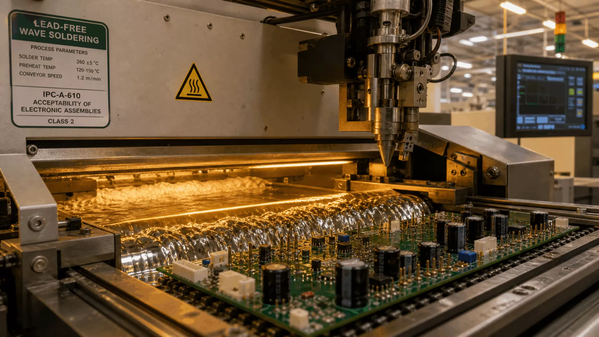
For boards with predominantly through-hole components on a single side, automated wave soldering delivers the highest throughput at the lowest per-joint cost. Our dual-wave systems — employing a turbulent primary wave for penetration into dense connector pin fields followed by a smooth secondary wave for fillet formation — process board widths up to 450 mm with conveyor speeds precisely controlled between 0.8 and 2.0 m/min. Pre-heat zones ramp the board to 100–130 degree Celsius before solder contact, minimizing thermal shock. Solder pot temperature is maintained at 260 plus minus 5 degree Celsius with automated dross removal. Nitrogen inerting is available for oxygen-sensitive assemblies, reducing dross formation by up to 80 percent and improving hole fill on high-aspect-ratio barrels.
Selective Soldering
When a board carries both surface-mount and through-hole components — or when through-hole parts appear on both sides — wave soldering is no longer viable. Selective soldering solves this by applying solder only to targeted through-hole sites using a programmable micro-fountain nozzle. ADD Components operates multi-axis selective soldering stations with nozzle diameters from 3 mm to 12 mm, capable of processing board sizes up to 508 x 508 mm. The system's integrated flux sprayer applies no-clean or water-soluble flux exclusively to the joint area, eliminating board-wide contamination. Thermal profiling is configured per component, with dwell times adjustable from 0.5 to 4.0 seconds per joint. This method is ideal for mixed-technology boards where SMT components on the bottom side cannot survive wave solder temperatures.
Manual Precision Soldering
For low-volume, high-complexity builds — or components requiring special handling such as heavy transformers, chassis-mounted connectors, and hand-wound magnetics — IPC-A-610-certified technicians perform manual soldering under stereo microscope magnification. Each station is equipped with temperature-controlled soldering irons calibrated daily to within plus minus 2 degree Celsius, fume extraction, and ESD-safe work surfaces. This capability also supports rework and repair of individual through-hole joints without exposing the entire board to reflow temperatures, preserving neighboring SMT devices from cumulative thermal stress.
| Process | Max Board Size | Typical Throughput | Best For |
|---|---|---|---|
| Wave Soldering | 450 x 500 mm | 60-120 boards/hr | Single-sided THT-heavy boards |
| Selective Soldering | 508 x 508 mm | 3-8 joints/sec | Mixed SMT/THT, double-sided THT |
| Manual Soldering | No practical limit | Application-dependent | Prototypes, heavy components, rework |
Component Sourcing: A Unified Supply Chain
One of the persistent pain points in through-hole assembly is component availability. Many through-hole parts — particularly connectors from TE Connectivity, Molex, Amphenol, and Hirose — carry lead times stretching to 26 weeks or longer during allocation periods. ADD Components mitigates this risk through its established position as a Hong Kong-based electronic components distributor. With direct relationships spanning STM, ADI, TI, Xilinx, Altera, Microchip, and dozens of connector and passive-component manufacturers, we can source the through-hole bill of materials alongside the PCB assembly order, collapsing two supplier relationships into one. This is particularly valuable for designs using legacy DIP-package ICs or specialized connectors that are not stocked by assembly-only providers.
Quality Verification and Compliance
Every through-hole assembly run undergoes inspection against the IPC-A-610 standard, with Class 2 and Class 3 acceptance criteria available depending on the end application. Automated optical inspection verifies component presence, orientation, and polarity on the topside. For wave-soldered and selectively-soldered joints, we perform cross-sectional analysis on sacrificial coupons to confirm barrel fill exceeding 75 percent — the Class 3 requirement. Solder fillet geometry on both primary and secondary sides is measured against the IPC-A-610 75-percent land-fill criterion. Where specified, ICT or flying-probe testing validates electrical continuity through every plated through-hole in the assembly.
For customers building products destined for industrial automation, railway signaling, medical devices, or aerospace ground-support equipment, this inspection regime provides the documented traceability required by ISO 9001 and related quality management frameworks. Board-level serialization with 2D data-matrix codes enables full lot-to-lot traceability from bare PCB fabrication through to final electrical test.
Submit your BOM and Gerber files to info@addcomponents.hk for a PCBA quotation — typically within 24 hours.