
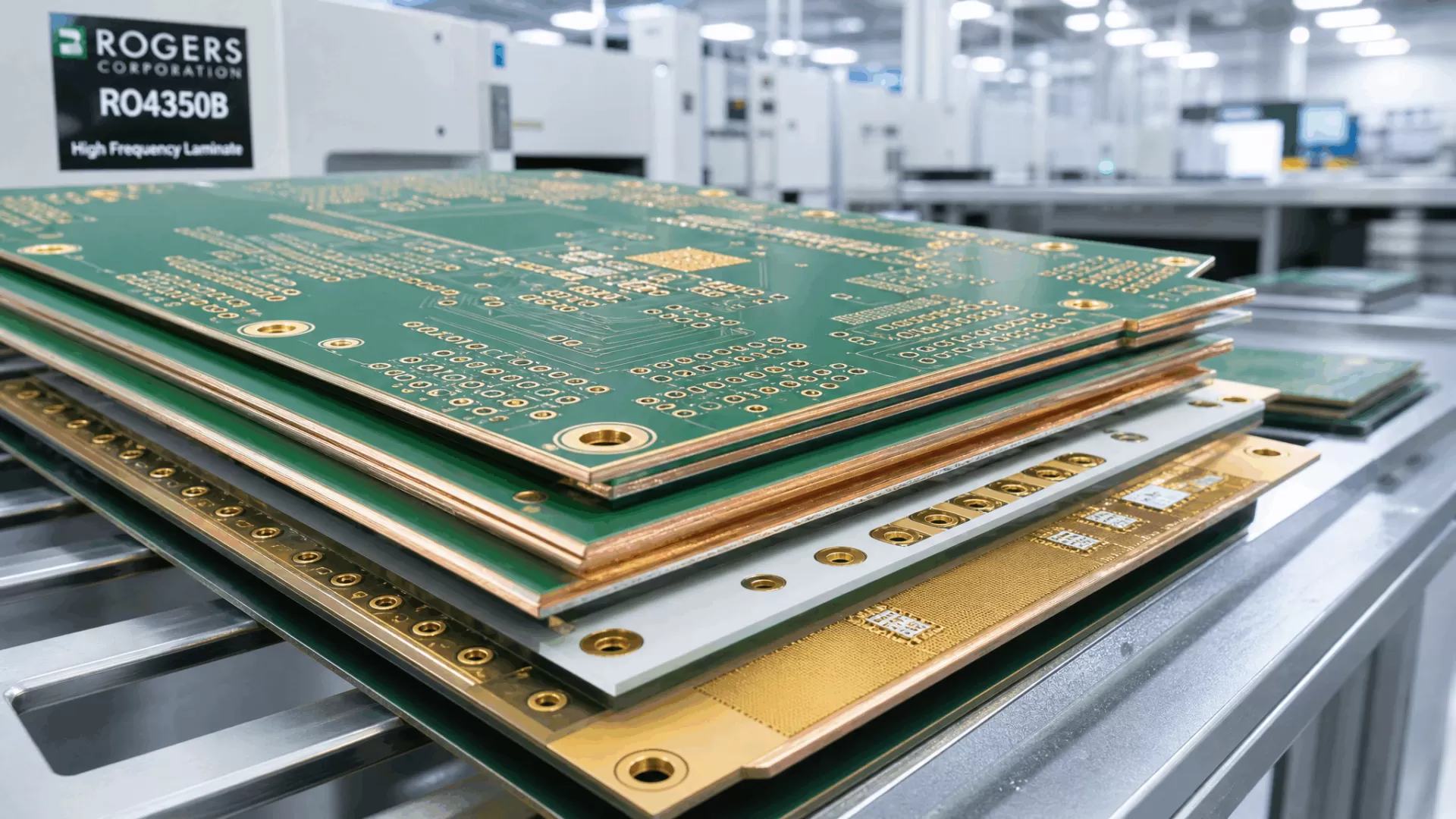
Printed circuit board fabrication sits at the intersection of electrical design intent and physical manufacturing reality. A board layout that looks correct in an EDA tool can fail dramatically in fabrication if the stackup, material selection, and process tolerances are not aligned with the manufacturer's actual capability. ADD Components bridges this gap by pairing design-for-manufacturability (DFM) review with fabrication partner selection across a network of qualified PCB suppliers — ensuring that the board delivered to the SMT line matches what the engineering team specified.
The Cost of Supplier Quality Inconsistency
One of the most common procurement frustrations in PCB fabrication is lot-to-lot variability: a prototype run that yields excellent results, followed by a production batch with registration errors, via quality issues, or solder mask misalignment. This inconsistency often traces back to fabricators that perform well within a narrow process window but lack the statistical process control to maintain quality across successive production runs. ADD Components qualifies fabrication partners against measurable criteria — including first-pass yield history, impedance control capability, and cross-section micrograph review — before routing any client design to production. This pre-qualification eliminates the trial-and-error cycle that costs engineering teams weeks of debugging.
Substrate Selection: Matching Material to Application
Material choice is the single most consequential decision in PCB fabrication. The substrate determines not only electrical performance — dielectric constant (Dk), dissipation factor (Df), thermal coefficient of dielectric constant — but also thermal reliability, moisture absorption, and long-term mechanical stability. ADD Components supports fabrication across the following substrate categories:
| Substrate Type | Typical Tg | Dk Range | Primary Applications |
|---|---|---|---|
| Standard FR-4 | 130–140°C | 4.2–4.6 | Consumer electronics, general digital, low-layer-count designs |
| High-Tg FR-4 | 170–180°C | 4.0–4.4 | Automotive, industrial controls, Pb-free reflow compatible designs |
| Rogers 4350B | >280°C | 3.48 ± 0.05 | RF/microwave, antenna arrays, power amplifiers above 500 MHz |
| Rogers 4003C | >280°C | 3.38 ± 0.05 | High-frequency digital, mmWave, satellite communications |
| Aluminum core (IMS) | N/A (metal base) | 4.0–8.0 (dielectric) | LED lighting, power converters, high-thermal-dissipation designs |
| Polyimide (flex) | >250°C | 3.2–3.5 | Wearable devices, dynamic flex applications, aerospace interconnects |
| Rigid-flex (FR-4 + polyimide) | Hybrid | Mixed | Medical devices, mil-aero, compact assembled enclosures |
For mixed-dielectric stackups — for example, a 12-layer board using Rogers 4350B on layers 1–2 for RF traces and FR-4 on layers 3–12 for digital routing — ADD Components coordinates with fabricators experienced in hybrid lamination to manage differential thermal expansion and avoid delamination during reflow.
Impedance Control: Tolerances That Matter
Impedance-controlled traces demand more than a fabricator entering trace width and spacing into a field solver. True impedance control requires monitoring the actual dielectric thickness and copper profile of every lamination cycle and adjusting line widths accordingly. ADD Components' fabrication partners routinely deliver single-ended impedance tolerance of ±10% and differential impedance tolerance of ±10% on standard FR-4 designs. For RF applications on Rogers substrates, tolerances tighten to ±7% or better. Each impedance-controlled order includes a TDR (Time Domain Reflectometry) test report with measured values for every controlled net, not just a statistical sample.
Supported impedance configurations include surface microstrip, edge-coupled differential microstrip, stripline (symmetric and asymmetric), and broadside-coupled differential pairs. Designs requiring 100-ohm differential (USB, Ethernet, LVDS) or 50-ohm single-ended (RF, DDR clock) are validated against the stackup before fabrication release.
Via Technology and High-Density Interconnect
Modern PCB designs increasingly rely on advanced via structures to escape high-pin-count BGAs and meet signal integrity requirements. ADD Components supports the full range of via technologies:
Through-hole vias: Standard mechanical drilling down to 0.20 mm diameter; aspect ratio up to 10:1
Blind vias: Laser-drilled microvias connecting outer layer to the next internal layer; minimum diameter 0.10 mm; used for BGA fanout and HDI stackups
Buried vias: Vias connecting internal layers without extending to outer surfaces; mechanically drilled or laser-formed depending on aspect ratio requirements
Stacked and staggered microvias: Multi-level HDI structures for 0.4 mm and 0.5 mm pitch BGA escape routing; stacked vias require copper-filled construction with planarization
Via-in-pad: Filled and plated-over vias placed directly in SMT pads for maximum routing density; conductive fill (copper) or non-conductive fill options available
Each via type carries distinct reliability implications. For example, stacked microvias at the interface between two HDI dielectric layers are susceptible to interfacial fracture under thermal cycling. ADD Components specifies staggered via patterns where possible and validates stacked structures against IPC-6016 Class 3 requirements when required for density reasons.
Copper Weight and Heavy Copper Capability
Standard PCB fabrication typically uses 0.5 oz (18 μm) or 1 oz (35 μm) copper on outer and inner layers. Power electronics, motor drives, and battery management systems often require substantially thicker copper to handle current without excessive I²R heating or voltage drop. ADD Components supports copper weights from 0.5 oz (18 μm) to 12 oz (420 μm) on outer layers and up to 6 oz (210 μm) on inner layers. Fabricators handling heavy copper must compensate for etch undercut — the lateral erosion of copper sidewalls during the etching process, which becomes proportionally larger as copper thickness increases — by adjusting trace width in the phototool artwork.
Surface Finishes and Final Plating
Surface finish selection balances solderability shelf life, coplanarity requirements, and cost. ADD Components offers the following finishes, each specified against IPC-4552 (ENIG), IPC-4554 (Immersion Tin), and IPC-4556 (ENEPIG) where applicable:
| Finish | Typical Thickness | Shelf Life | Best For |
|---|---|---|---|
| ENIG (Electroless Nickel Immersion Gold) | 3–6 μm Ni / 0.05–0.12 μm Au | 12 months | Fine-pitch BGA, wire bonding, general-purpose SMT |
| HASL (Hot Air Solder Leveling) | 1–40 μm (uneven) | 12 months | Through-hole, coarse-pitch SMT, cost-sensitive designs |
| Lead-free HASL | 1–40 μm (uneven) | 12 months | RoHS-compliant, same applications as HASL |
| OSP (Organic Solderability Preservative) | 0.2–0.5 μm | 6 months | Fine-pitch SMT, single-sided reflow, short shelf-life acceptable |
| Immersion Silver | 0.15–0.40 μm | 6–12 months | RF/microwave (low insertion loss), high-frequency digital |
| Immersion Tin | 0.8–1.2 μm | 6 months | Press-fit connectors, flat surface requirement |
ENIG is the default recommendation for fine-pitch components below 0.5 mm pitch due to its flat surface profile and excellent wire-bonding compatibility. For RF designs, Immersion Silver is preferred because its thin, uniform coating minimizes conductor loss at microwave frequencies.
From Gerber Review to Fabrication Release
ADD Components performs a DFM check on every set of Gerber files before release to fabrication. The review covers annular ring adequacy, solder mask sliver detection, copper-to-edge clearance, drill-to-copper spacing, and impedance stackup consistency. Any DFM flags are reported back to the client with recommended corrective actions — typically within one business day for standard stackups. Once approved, the fabrication order proceeds with a confirmed lead time that accounts for the layer count, substrate availability, and finishing process. Prototype quantities of 5–100 pieces can be delivered in as few as 5–7 working days for standard 2–8 layer FR-4 designs; complex 16+ layer Rogers or rigid-flex stackups typically require 10–18 working days.
Submit your BOM and Gerber files to info@addcomponents.hk for a PCBA quotation — typically within 24 hours.